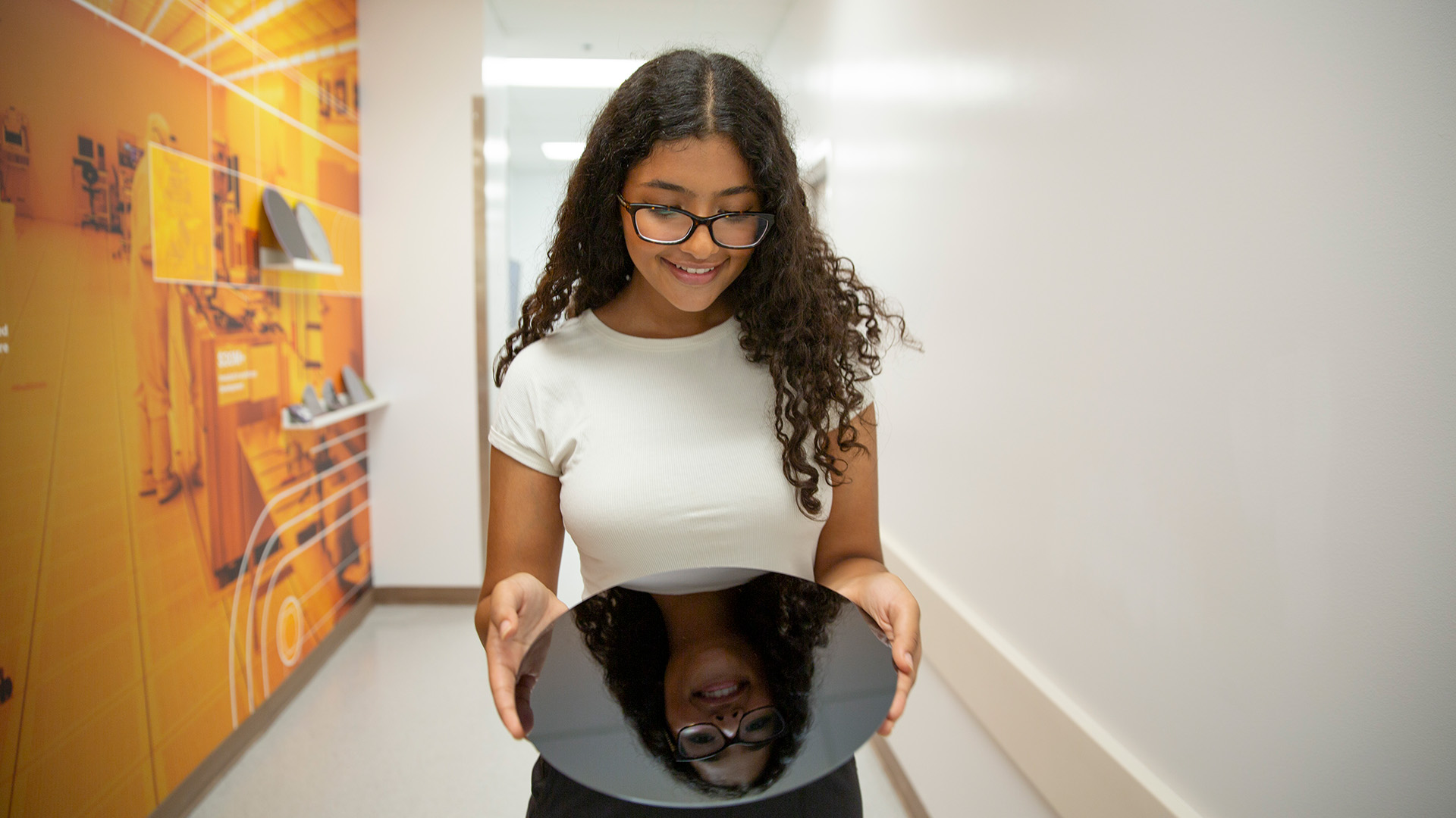
Sidra Elsaady
Engineering (electrical systems)
Hometown: Cairo, Cairo, Egypt
Graduation date: Spring 2028
FURI | Fall 2025
Evaluating UV Ozone vs. Open-Air Plasma Comparisons for Underfill Effectiveness
Underfill materials are essential in semiconductor packaging, as they reinforce mechanical stability and protect solder joints from thermal and mechanical stress. Semiconductor surfaces are typically treated to improve adhesion and activation for reliable underfill bonding. UV ozone is commonly used for this surface activation, but open-air plasma may provide a more scalable and cost-effective alternative. In this study, silicon substrates coated with a tin oxide layer are treated using both methods and evaluated through profilometry, contact angle measurements, and adhesion testing to determine which provides better surface conditioning.
Mentor: Nick Rolston

It’s hip to be square.
Students presenting projects at the Fulton Forge Student Research Expo are encouraged to download this personal QR code and include it within your poster. This allows expo attendees to explore more about your project and about you in the future.
Right click the image to save it to your computer.
Featured project | Fall 2025
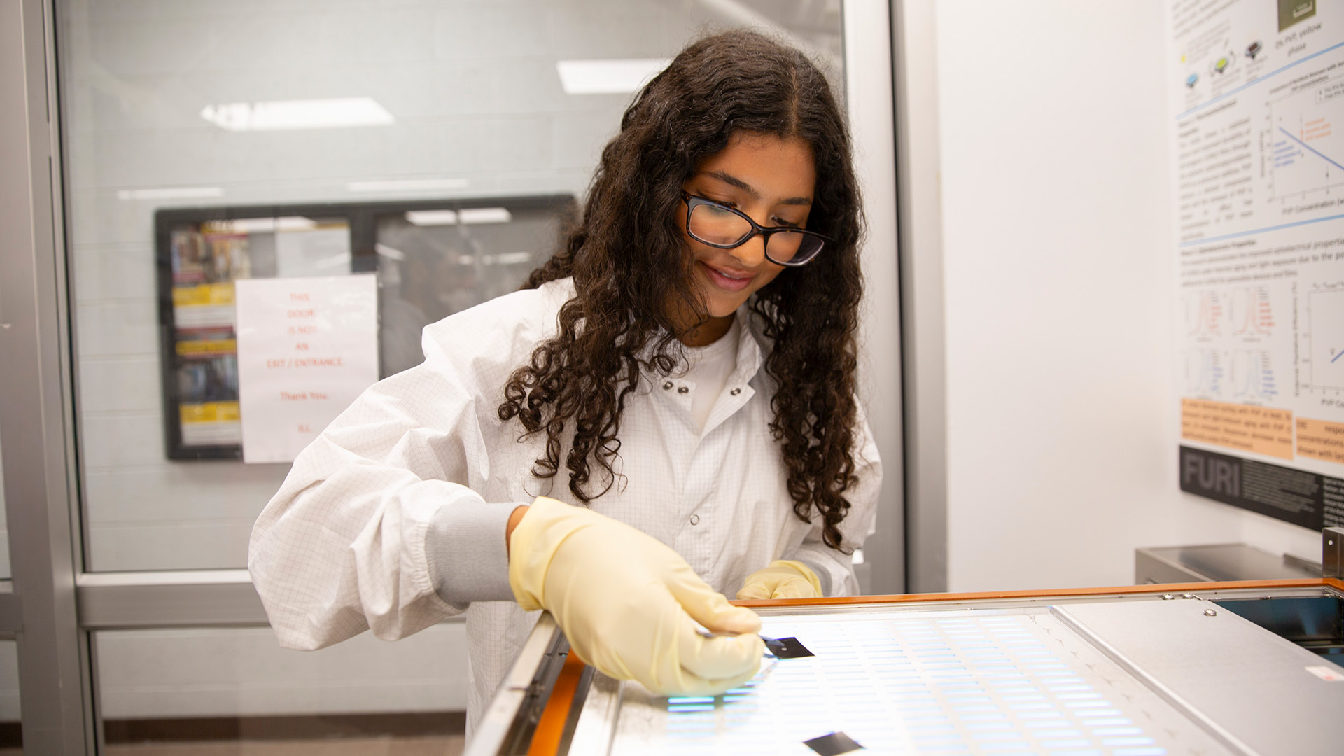
Sidra Elsaady, an undergraduate engineering student specializing in electrical systems engineering, decided to join FURI to see how the theoretical concepts she was learning in her classes applied to the real world. Supervised by Nick Rolston, a Fulton Schools assistant professor of electrical engineering, Elsaady is testing different treatment methods’ effects on semiconductor device packaging quality to improve the reliability of electronics.
What made you want to get involved in this program? Why did you choose the project you’re working on?
I joined this program because I really wanted to take what I was learning in electrical systems engineering and see how it works in the real world. I’ve always liked connecting the science side of things with the hands-on engineering side, and this project gave me that chance. Honestly, a big part of it was just wanting to be in a real lab for the first time, not just classroom labs where everything is already set up for you. Being surrounded by the equipment and learning how to actually use it was something I’d been curious about for a long time. I also wanted to figure out if research was something I’d truly enjoy, and this felt like the perfect way to test that. It turns out I love it; the mix of problem solving, experimenting and learning new processes in semiconductor manufacturing has been really motivating.
How will your engineering research project impact the world?
What I really like about this project is that it shows how even the smallest details in engineering can completely change the performance of something as big as a semiconductor device. I’m testing different treatments like vacuum-based plasma, open-air plasma and ultraviolet-ozone, to see how they affect surface roughness, wettability and other key properties in packaging. These aren’t just random measurements; they’re what make the difference between a device that lasts for years and one that fails too soon. If treatments like open-air plasma or ultraviolet-ozone can work as well as or even better than traditional vacuum systems, that could mean more efficient, lower-cost and more sustainable manufacturing.
What has been your most memorable experience as a student researcher in this program? Did you have a particular “aha!” moment during your project?
My most memorable experience has been getting trained on the equipment and realizing I was finally working in a real research lab. Before this, most of my lab work had been in classroom settings where the experiments were already planned out and very controlled. Walking into a research lab felt completely different. The scale, the freedom and the advanced equipment for plasma treatments, profilometry and more made me feel like I was stepping into the world of real engineering. Being able to actually use the equipment myself and learn how different experiments are run was motivating and exciting. It showed me how much more there is to explore in semiconductor research and made me want to keep building my skills and stay curious about everything this field has to offer.
How do you see this experience helping with your career or advanced degree goals?
This project has helped me realize how much I enjoy doing research. Before starting, I wasn’t sure if research was the right fit for me, but being in the lab and working through experiments showed me that this is something I want to keep doing. I’d like to continue my research in this field, and then branch out into more areas of semiconductor research over time. The skills I’ve gained are things I can carry with me, whether I go into industry or pursue an advanced degree. More importantly, this experience confirmed that I want to keep building on what I’ve started, and I see it as the beginning of a longer journey into semiconductor manufacturing and processing.
Why should other students get involved in this program?
Other students should get involved in this program because it gives you the freedom to explore areas of research you wouldn’t normally get to dive into as an undergraduate. You can start your own project or join an existing one, which means you can really shape the experience to your interests. It’s not just about the material you cover in class; you get the chance to explore topics and ask questions that would never even come up in a regular lecture, and you get to apply that knowledge in real ways through your own project. For me, this program confirmed how much I enjoy research, but it’s also a great way for any student to figure out whether research is something they want to keep pursuing. Even if you end up in a completely different field, the experience of working in a real lab, gaining technical skills and taking ownership of a project sets you apart and gives you a perspective you can’t get from the classroom alone. It’s a chance to explore new topics, grow as an engineer, and find out what excites you most.